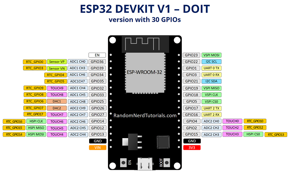
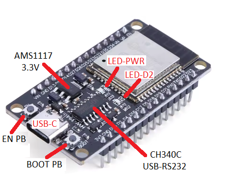
I got this module from AliExpress from a here-today-gone-tomorrow vendor with the development board with Dupont sockets and screw-down blocks for each pin. Total of about $7 for the pair. It looks like a nice development setup that I won’t lose sleep if I bury the development board in the final device.

Pinout Notes
| GPIO | Input | Output | Notes |
| 0 | Pulled up | OK | Outputs PWM signal at boot, must be LOW to enter flashing mode, strapping pin. |
| 1 | TX pin | OK | Debug output at boot |
| 2 | OK | OK | Connected to on-board LED, must be left floating or LOW to enter flashing mode, strapping pin. |
| 3 | OK | RX pin | HIGH at boot |
| 4 | OK | OK | |
| 5 | OK | OK | Outputs PWM signal at boot, strapping pin |
| 12 | OK | OK | Boot fails if pulled high, strapping pin. |
| 13 | OK | OK | |
| 14 | OK | OK | Outputs PWM signal at boot |
| 15 | OK | OK | Outputs PWM signal at boot, strapping pin |
| 16 | OK | OK | Lower output source current. Note 1 – DC Characteristics |
| 17 | OK | OK | Lower output source current. Note 1 – DC Characteristics |
| 18 | OK | OK | |
| 19 | OK | OK | |
| 21 | OK | OK | Default SDA. |
| 22 | OK | OK | Default SDL. |
| 23 | OK | OK | |
| 25 | OK | OK | Also 8-bit DAC1. |
| 26 | OK | OK | Also 8-bit DAC2. |
| 27 | OK | OK | |
| 32 | OK | OK | |
| 33 | OK | OK | |
| 34 | OK | Input only – No PUP/PUD | |
| 35 | OK | Input only – No PUP/PUD | |
| 36 | OK | Input only – No PUP/PUD | |
| 39 | OK | Input only – No PUP/PUD |
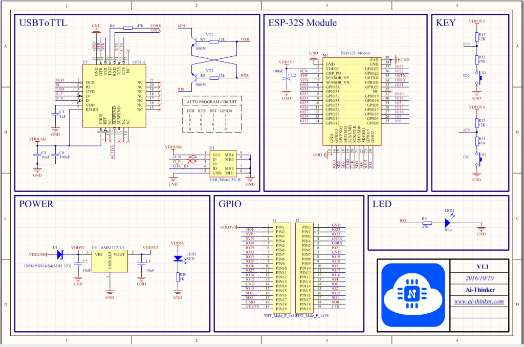
Typical Module Schematics
The actual ESP32 module may not uses the following schematics – but it should be pretty close. This schematic is specifically designed to support the WSP-32S (38 pin module). Just ignore the unsupported pins on your module.

Module Physical Layout

Strapping Pins
There are five pins that are required to be Hi-Z or open circuited when the ESP powers on (power-on-reset, RTC watchdog reset and brownout reset). Internally, the module uses internal pull-up and pull-down circuits to configure:
- Voltage of Internal LDO (VDD_SDIO) is 3.3V. The module integrates a 3.3 V SPI flash, so the pin cannot be set to 1 when the module is powered up.
- SPI Boot Mode
- Enable Debugging Log Print over U0TXD During Booting (GPIO1)
- Timing of SDIO Slave, RE Sampling, RE Output
CPU and Internal Memory
ESP32-D0WDQ6 contains two low-power Xtensa® 32-bit LX6 microprocessors. The internal memory includes:
- 448 KB of ROM for booting and core functions.
- 520 KB of on-chip SRAM for data and instructions.
- 8KB of SRAM in RTC, which is called RTC FAST Memory and can be used for data storage; it is accessed by the main CPU during RTC Boot from the Deep-sleep mode.
- 8KB of SRAM in RTC, which is called RTC SLOW Memory and can be accessed by the co-processor during the Deep-sleep mode.
- 1Kbit of eFuse: 256 bits are used for the system (MAC address and chip configuration) and the remaining.
- 768 bits are reserved for customer applications, including flash-encryption and chip-ID.
DC Characteristics
- Cin (Pin capacitance): 2 pf (typ)
- *** INPUT ***
- VIH (High level input voltage): 0.75xVDD (min), VDD+0.3 (max), V
- VIL (Low level input voltage): -0.3 (min), 0.25xVDD (max), V
- IIH, IIL (High level, low level input current): 50 nA (max)
- *** OUTPUT ***
- VOH (High level output voltage): 0.8xVDD (min), V
- VOL (Low level output voltage): 0.1xVDD (max), V
- IOH (High level source current): 40 mA (typ)
- IOH (High level source current, VDD_SDIO power domain): 20 mA (typ) Note 1
- IOL (Low level sink current, output drive strength set to maximum): 28 mA (typ)
Note 1 Pins in the VDD_SDIO power domain are designed to deliver less source power. They are typically used to power built-in FLASH or PSRAM since the voltage must be correct for the ICs used. Pins are as follows:
- GPIO16
- GPIO17
- Six others not exposed to external pins on this device.
